Table of Contents
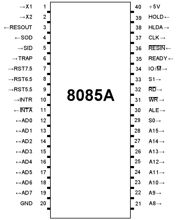
Toggle8085 Microprocessor has 40 pins and is used in many applications such as embedded systems, digital signal processing, and control systems. The pin diagram of 8085 microprocessor and function of each pin is discussed in this article.
Pin Diagram of 8085 Microprocessor
8085 is a 40 pin IC, DIP package. The pins of the 8085 microprocessor can be divided into six categories based on their function as follows:
- Power supply and clock signals
- Address bus
- Data bus
- Control and status signals
- Interrupts and externally initiated signals
- Serial I/O ports

Pin Description of 8085 Microprocessor
Power supply and Clock frequency signals:
- Vcc: This pin provides a +5V power supply to the microprocessor.
- Vss (or GND): This pin is the ground pin.
- CLK (out): Clock Output is used as the system clock for peripheral and devices interfaced with the microprocessor.
- X1, X2:
- Crystal or R/C network or LC network connections to set the frequency of internal clock generator.
- The frequency is internally divided by two. Since the basic operating timing frequency is 3 MHz, a 6 MHz crystal is connected externally.
Address Bus:
- A8 – A15 (output; 3-state)
- It carries the most significant 8 bits of the memory address or the 8 bits of the I/O address.
Multiplexed Address / Data Bus:
- AD0 – AD7 (input/output; 3-state)
- These multiplexed set of lines used to carry the lower order 8-bit address as well as data bus.
- During the opcode fetch operation, in the first clock cycle, the lines deliver the lower order address A0 – A7.
- In the subsequent IO / memory, read / write clock cycle the lines are used as data bus.
- The CPU may read or write out data through these lines.
Control and Status signals:
- ALE (output) – Address Latch Enable: This signal helps to capture the lower order address presented on the multiplexed address / data bus.
(output 3-state, active low)- Read memory or IO device: This indicates that the selected memory location or I/O device is to be read and that the data bus is ready for accepting data from the memory or I/O device.
(output 3-state, active low) – Write memory or IO device: This indicates that the data on the data bus is to be written into the selected memory location or I/O device.
(output) – Select memory or an IO device: This status signal indicates that the read / write operation relates to whether the memory or I/O device. It goes high to indicate an I/O operation. It goes low for memory operations.
Status Signals (S0,S1):
- It is used to know the type of current operation of the microprocessor.
- On receipt of an interrupt, the microprocessor acknowledges the interrupt by the active low INTA (Interrupt Acknowledge) signal.
- Table: Status signals and the status of data bus
S1
S0
Data Bus Status
0
0
0
Halt
0
0
1
Memory write
0
1
0
Memory read
0
1
1
Opcode fetch
1
0
1
I/O write
1
1
0
I/O read
1
1
1
Interrupt
acknowledge
Reset In (input, active low)
- This signal is used to reset the microprocessor.
- The program counter inside the microprocessor is set to zero.
- The buses are tri-stated.
Reset Out (Output)
- It indicates CPU is being reset.
- Used to reset all the connected devices when the microprocessor is reset.
READY (input)
- Memory and I/O devices will have slower response compared to microprocessors.
- Before completing the present job such a slow peripheral may not be able to handle further data or control signal from CPU.
- The processor sets the READY signal after completing the present job to access the data.
- The microprocessor enters into WAIT state while the READY pin is disabled.
Interrupts and externally initiated signals:
- As the name suggests this control interrupts a process. Consider that a microprocessor is executing the main program.
- Now whenever the interrupt signal is enabled or requested the microprocessor shifts the control from main program to process the incoming request and after the completion of request, the control goes back to the main program.
- For example, an Input/output device may send an interrupt signal to notify that the data is ready for input. The microprocessor temporarily stops the execution of main program and transfers control to I/O device.
- After collecting the input data, the control is transferred back to main program.
- Interrupt signals present in 8085 are:
- INTR
- RST 7.5
- RST 6.5
- RST 5.5
- TRAP
INTR is maskable 8080A compatible interrupt. When the interrupt occurs the processor fetches from the bus one instruction, usually one of these instructions: One of the 8 RST instructions (RST0 – RST7).
The processor saves current program counter into stack and branches to memory location N * 8 (where N is a 3 – bit number from 0 to 7 supplied with the RST instruction).
CALL instruction (3-byte instruction). The processor calls the subroutine, address of which is specified in the second and third bytes of the instruction.
RST5.5 is a maskable interrupt. When this interrupt is received the processor saves the contents of the PC register into stack and branches to 2CH (hexadecimal) address.
RST6.5 is a maskable interrupt. When this interrupt is received the processor saves the contents of the PC register into stack and branches to 34H (hexadecimal) address.
RST7.5 is a maskable interrupt. When this interrupt is received the processor saves the contents of the PC register into stack and branches to 3CH (hexadecimal) address.
TRAP is a non-maskable interrupt. When this interrupt is received the processor saves the contents of the PC register into stack and branches to 24H (hexadecimal) address.
All maskable interrupts can be enabled or disabled using EI and DI instructions. RST5.5, RST6.5 and RST7.5 interrupts can be enabled or disabled individually using SIM instruction.
Single Bit Serial I/O ports:
- SID (input) – Serial input data line
- SOD (output) – Serial output data line
- These signals are used for serial communication.
Recent posts
Related posts:
- Terminology Used in Microprocessor and Microcontroller
- CISC and RISC Processor Architecture
- Von Neumann and Harvard Architecture
- Basics of Microprocessor and Microcontroller
- Introduction to Microprocessor 8085
- Architecture of 8085 Microprocessor
- Addressing Modes in 8085 Microprocessor
- Data Transfer Instructions in 8085 Microprocessor
- Arithmetic Instructions in 8085 Microprocessor
- Logical Instructions in 8085 Microprocessor
- Branching instructions in 8085 Microprocessor
- Machine Control Instructions in 8085 Microprocessor
- Timing Diagram of 8085 Instructions
- Stack and Subroutine in 8085 Microprocessor
- Interrupts in 8085 Microprocessor
- Assembler Directives of 8085 Microprocessor
- Simple Data Transfer Program in 8085 Microprocessor
- Microprocessor 8085 Addition and Subtraction Programs
- Programs on Logical Instructions in 8085 Microprocessor
- Multiplication Programs in 8085 Microprocessor
- Division Programs in 8085 Microprocessor
- Introduction to Assembly Language Programming
- 8085 Program to Find the Largest Number in an Array of Data
- 8085 Program to Count Negative Numbers | ALP to Count Negative Numbers
- 8085 Program to Find the Smallest Number in An Array of Data
- 8085 Program to Arrange an Array of Data in Ascending Order
- 8085 Program to Arrange an Array of Data in Descending Order
- 8085 Program to Find the Square of a Number from 0 to 9 Using a Table of Square


