Table of Contents
ToggleSumming amplifiers or adders are the amplifier circuits which can add more than one input signal. It is possible to apply more than one input signal to an inverting or non-inverting terminal of op-amp.
The summing amplifier then add all these input signals to produce their addition at the output.
Depending on the polarity of the output voltage the adder circuit can be classified into two categories as
- Inverting summing amplifier
- Non-inverting summing amplifier
Inverting Summing Amplifier Using Op-Amp
The summing amplifier is same as that inverting amplifier except that is has several input terminals. The negative feedback applied through resister Rf from the output to the input terminal.
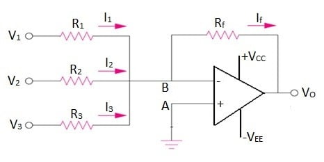
Following figure shows the circuit diagram of an inverting configuration of summing amplifier (Inverting adder) using op-amp.

As shown in figure, the input voltages V1, V2 and V3 are applied through resistance R1, R2 and R3 respectively to the inverting terminal of op-amp.
Let the current flowing through resistance R1, R2 and R3 be I1, I2 and I3 respectively.
Let VA is the voltage at non-inverting terminal and VB is the voltage at inverting terminal respectively.
Applying Kirchhoff’s current law (KCL) at node B,
(KCL: Sum of current going toward node is equal to sum of currents going away from the node.)
…(1)
According to the concept of virtual ground, as node A is grounded, node B is also grounded, i.e., VA= VB= 0,
Putting VB= 0 in equation (1) we get
…(2)
Therefore, equation (2) will become
…(3)
Where R1≠R2≠R3
It is known as “scaling amplifier” or “Weighted amplifier”.
If Rf=R1=R2=R3=R then,
we get,
This circuit is called as “Inverting Adder” or “Inverting Summing Amplifier”.
If R1=R2=R3=R and Rf =Ri/3
Equation (3) becomes,
Thus, the magnitude of output voltage is equal to the average of three input voltages. This is called “Averaging amplifier”.
Non-inverting Summing Amplifier Using Op-Amp
Non-inverting Summing Amplifier or non-inverting adder is the circuit in which the output is proportional to the sum of the input and also the output is in phase with input.
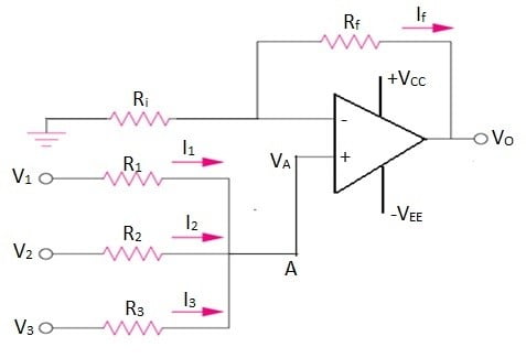
The negative feedback applied through resister Rf from the output to the input terminal. Following figure shows the circuit diagram of non-inverting configuration of summing amplifier (non-inverting adder) using op-amp.

As shown in figure, the input voltages V1, V2 and V3 are applied through resistance R1, R2 and R3 respectively to the non-inverting terminal of op-amp.
Let the current flowing through resistance R1, R2 and R3 be I1, I2 and I3 respectively.
Let VA is the voltage at non-inverting terminal.
Applying Kirchhoff’s current law (KCL) at node A,
(KCL: Sum of current going toward node is equal to sum of currents going away from the node.)
Also,
Above equation can be rearranged as
…(4)
Let R1=R2=R3=R;
Equation (4) will become,
…(5)
But for non-inverting amplifier output voltage is given by
As input voltage at non-inverting terminal is Vin = VA,
…(6)
From equation (5) and (6),
…(7)
To make output voltage as sum of all input voltages (V1+V2+V3),
Therefore, equation (7) becomes,


