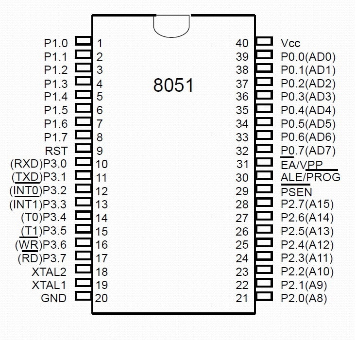
The 8051 microcontroller is packaged in 40 pin dual in line package (DIP). Out of 40 pins, 16 pins are single function pins and 24 pins may be used for one or two entirely different function.
The pin configuration of 8051 microcontroller is as follows.

Out of 32 I/O lines of four ports, 8 lines of port 1 are used as single I/O function only. The remaining 24 pins of port 0, port 2 and port 3 are used for dual functions.
Port 0 pins used for I/O function and lower address and data multiplexed port for external memory. Port 2 pins used for I/O function and higher address for external memory. Port 3 pins used for I/O functions and Alternative uses.
Pin Functions of 8051
Pins 1-8: Port 1 Each of these pins can be configured as an input or an output.
Pin 9: RST
- It is an active high input pin and normally low. Upon applying a high pulse to this pin, 8051 terminate all activities and go to reset condition. By applying logic zero to this pin, the program starts execution from the beginning.
- 8051 responds to an RST high input only if the RST is held high for at least two machine cycles.
- A machine cycle is the period taken by any processor to fetch and execute one instruction.
- In 8051, the maximum number of clock cycles taken for a machine cycle is 12. So, the RST pin must be high for at least 24 clock periods.
Pins10-17: Port 3
Similar to port 1, each of these pins can serve as general input or output. Besides, all of them have alternative functions:
- Pin 10: RXD Serial asynchronous communication input or Serial synchronous communication output.
- Pin 11: TXD Serial asynchronous communication output or Serial synchronous communication clock output.
- Pin 12:
Interrupt 0 input. - Pin 13:
Interrupt 1 input. - Pin 14: T0 Counter 0 clock input.
- Pin 15: T1 Counter 1 clock input.
- Pin 16:
Write to external (additional) RAM. - Pin 17:
Read from external RAM.
Pin 18, 19: X2, X1
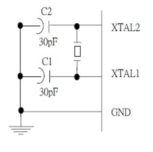
- The 8051 has an on-chip oscillator but requires an external crystal to run it.
- A quartz crystal oscillator is connected to inputs XTAL1 (pin19) and XTAL2 (pin18).
- The quartz crystal oscillator also needs two capacitors of 30 pF value. The original 8051 operates at 12 MHz.
- The crystal frequency determines the basic clock frequency of 8051. A quartz crystal which specifies operating frequency is usually connected to these pins.

- If you use a frequency source other than a crystal oscillator, such as a TTL oscillator. It will be connected to XTAL1 and XTAL2 is left unconnected.

Pin 20: GND Ground.
Pin 21-28: Port 2
- If there is no intention to use external memory then these port pins are configured as general inputs/outputs.
- In case external memory is used, the higher address byte, i.e. addresses A8-A15 will appear on this port.
- Even though memory with capacity of 64Kb is not used, which means that not all eight port bits are used for its addressing, the rest of them are not available as inputs/outputs.
Pin 29: (Program Store Enable)
- The read strobe to external program memory.
- If external ROM is used for storing program then a logic zero (0) appears on it every time the microcontroller reads a byte from memory.
- When executing code from the external program memory, it is activated twice each machine cycle, except that two
activations are skipped during each access to external data memory.
Pin 30: ALE
- Prior to reading from external memory, the microcontroller puts the lower address byte (A0-A7) on P0 and activates the ALE output.
- After receiving signal from the ALE pin, the external register (usually 74HCT373 or 74HCT375 add-on chip) memorizes the state of P0 and uses it as a memory chip address. Immediately after that, the ALU pin is returned its previous logic state and P0 is now used as a Data Bus.
- As seen, port data multiplexing is performed by means of only one additional (and cheap) integrated circuit. In other words, this port is used for both data and address transmission.
Pin 31:
- By applying logic zero to this pin, P2 and P3 are used for data and address transmission with no regard to whether there is internal memory or not.
- It means that even there is a program written to the microcontroller, it will not be executed. Instead, the program written to external ROM will be executed.
- By applying logic one to the EA pin, the microcontroller will use both memories, first internal then external (if exists).
Pin 32-39: Port 0
- Similar to P2, if external memory is not used, these pins can be used as general inputs/outputs.
- Otherwise, P0 is configured as address output (A0-A7) when the ALE pin is driven high (1) or as data output (Data Bus) when the ALE pin is driven low (0).
Pin 40: VCC +5V power supply.


