Table of Contents
ToggleAll 8051 microcontrollers have 4 I/O ports each comprising 8 bits which can be configured as inputs or outputs. The four ports are port 0, port 1, port 2 and port 3. Lets understand the functions of ports in 8051 microcontroller.
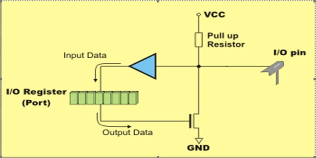
Each port is 8-bit port having 8 pins and has D-type o/p latch for each pin. Accordingly, in total of 32 input/output pins enabling the microcontroller to be connected to peripheral devices are available for use.
Input/Output Pins and Ports
- The Special Function Register (SFR) for each port is made up of these eight latches, which can be address for that port. The port latches should not be confused with the port pins.
- The data in the latches does not have to be the same as that on port pins. The data in latch buffer and the data of ports pins can be read independently.
- Pin configuration, i.e. whether it is to be configured as an input or an output, depends on its logic state.
- In order to configure a microcontroller pin as an output, it is necessary to apply a logic zero (0) to appropriate I/O port bit. In this case, voltage level on appropriate pin will be 0.
- Similarly, in order to configure a microcontroller pin as an input, it is necessary to apply a logic one (1) to appropriate port. In this case, voltage level on appropriate pin will be 5V (as is the case with any TTL input).
- By default, the port is defined as output port.
Port 0
- The P0 port is characterized by two functions. If external memory is used then the lower address byte (addresses A0-A7) is applied on it. Otherwise, all bits of this port are configured as inputs/outputs.
- The other function is expressed when it is configured as an output. Unlike other ports consisting of pins with built-in pull-up resistor connected by its end to 5V power supply, pins of this port have this resistor left out. This apparently small difference has its consequences:

- If any pin of this port is configured as an input then it acts as if it “floats”. Such an input has unlimited input resistance and undetermined potential.
- When the pin is configured as an output, it acts as an “open drain”.

- By applying logic 0 to a port bit, the appropriate pin will be connected to ground (0V).
- By applying logic 1, the external output will keep on “floating”. In order to apply logic 1 (5V) on this output pin, it is necessary to built in an external pull-up resistor.
Note: Only in case P0 is used for addressing external memory, the microcontroller will provide internal power supply source in order to supply its pins with logic one. There is no need to add external pull-up resistors.
Port 1
- P1 is a true I/O port, because it doesn’t have any alternative functions as is the case with P0, but can be configured as general I/O only.
- It has a pull-up resistor built-in and is completely compatible with TTL circuits.

Port 2
- P2 acts similarly to P0 when external memory is used. Pins of this port occupy addresses intended for external memory chip. This time it is about the higher address byte with addresses A8-A15.
- When no memory is added, this port can be used as a general input/output port showing features similar to P1.
Port 3
- All port pins can be used as general I/O, but they also have an alternative function. In order to use these alternative functions, a logic one (1) must be applied to appropriate bit of the P3 register.
- In terms of hardware, this port is similar to P0, with the difference that its pins have a pull-up resistor built-in.
- The alternate function of each pin of port 3 is as follows.
PORT 3 Pin | Alternate Function | Description |
P3.0 | RXD | Serial input data |
P3.1 | TXD | Serial output data |
P3.2 | INT0 | External interrupt 0 |
P3.3 | INT1 | External interrupt 1 |
P3.4 | T0 | External timer 0 clock |
P3.5 | T1 | External timer 1 clock |
P3.6 | WR | External memory write enable |
P3.7 | RD | External memory read enable |
Recent posts
Related posts:
- Assembler Directives in 8051 Microcontroller
- Features of 8051 Microcontroller
- Memory Organization of 8051 Microcontroller
- Addressing Modes in 8051 Microcontroller
- Instruction Set in 8051 Microcontroller
- Architecture of 8051 Microcontroller
- PSW Register in 8051 Microcontroller | Program Status Word
- Pin Configuration of 8051 Microcontroller
- The Stack and Stack Pointer in 8051 Microcontroller
- Stack Pointer Data Pointer and Program Counter in 8051 Microcontroller
- Functions of Timing and Control Unit of 8051


I think this is one of the most important information for me.
And i’m glad reading your article. But should remark on some general things,
The web site style is great, the articles is really
excellent : D. Good job, cheers