Table of Contents
ToggleClosed Loop Configuration
When a part of output is fed back (given) to the input it is called closed loop configuration. It means that some kind of feedback is introduced in the circuit. In this article, following four circuits of closed loop configuration of Op-amp are explained.
- Inverting amplifier
- Sign changer
- Non-inverting amplifier
- Voltage follower
Inverting Amplifier
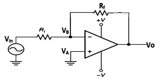
In this mode of an Op-amp, non-inverting terminal is grounded and the input voltage (Vin) is applied to inverting terminal through resistor Ri. The negative feedback is applied through resistor Rf from output to input.
For amplification feedback resistance must be greater than input resistance (Rf > Ri).
The circuit diagram for closed loop inverting configuration of op-amp (Inverting amplifier) is as follows.
Expression for Output Voltage
Let the voltage at point A and B is VA and VB respectively.
Applying Kirchhoff’s current law at point B,
…(1)
As node A is grounded. Considering Op-amp as ideal, node B is at virtual ground. (Always apply virtual ground concept to inverting configuration of op-amp.)
VA=VB=0
…(2)
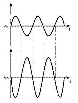
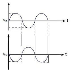
This is expression for output voltage of closed loop inverting amplifier. The negative sign indicates that there is a phase shift of 180° between the input and output voltages.
Similarly, using above equation (2) the gain can be given as
Here
is closed loop gain for inverting Op-amp. Here negative sign indicates input is inverted at output. Hence it is called as inverting amplifier.
Output Waveform of Inverting Amplifier
Inverter or Sign-Changer
In a closed loop inverting amplifier if
Rf=Ri=R then
Gain = -1
The circuit diagram for Op-amp as an inverter is as follows.
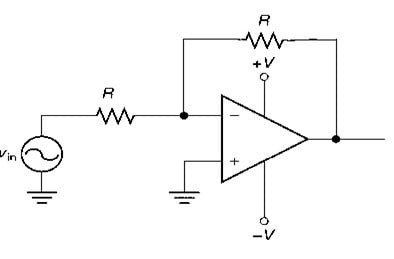
The output equals to input with 180° out of phase in inverter or sign changer.
Non-Inverting Amplifier
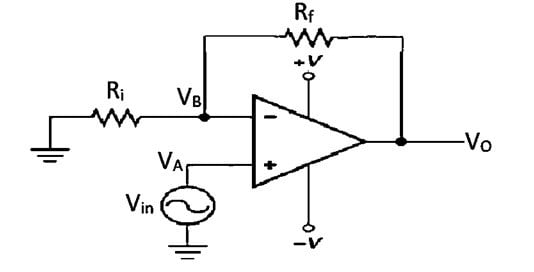
In this mode of an Op-amp, the inverting terminal is grounded and the input voltage (Vin) is applied to non-inverting terminal through resistor Ri. The negative feedback is applied through resistor Rf from output to input.
For amplification feedback resistance must be greater than input resistance (Rf > Ri).
The circuit diagram for closed loop non-inverting configuration of op-amp (Non-inverting amplifier) is as follows.
Expression for Output Voltage
Let the voltage at point A and B is VA and VB respectively.
Applying Kirchhoff’s current law at point B,
… (1)
Consider Op-amp as an ideal Op-amp. As node A is at potential Vin, the node B is also at same potential.
Hence equation (1) will be
… (2)
This is expression for output voltage of a non-inverting amplifier.
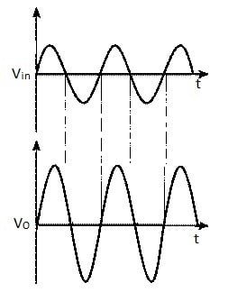
There is no negative sign indicates that the output voltage and input voltage are in phase. As input voltage is not inverted at output, it is called as non-inverting amplifier.
Now, the gain of non-inverting op-amp can be obtained by using equation (2) as
Here is closed loop gain for non-inverting Op-amp.
Output Waveform of Non-Inverting Amplifier
Voltage Follower (Unity Gain Buffer)
When Ri=∞ and Rf=0 the non-inverting amplifier gets converted into voltage follower or unity gain amplifier.
The circuit diagram of Op-amp as an unity gain follower (Voltage follower) is as follows.
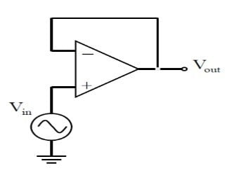
A circuit in which the output voltage follows the input voltage is called follower circuit.
For non-inverting amplifier,
As Rf=0 means no feedback is present
Gain=1
Here output voltage will be equal and in phase with input voltage.


